|
Article (English)  Top
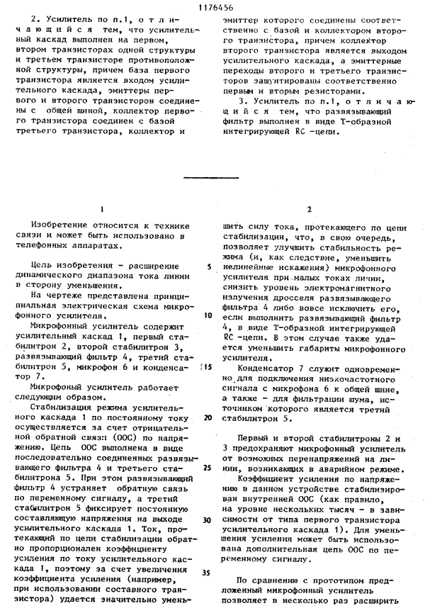
Top
SEMICONDUCTOR ELECTRONICS IN COMMUNICATIONS
Article Digest
Edited by I.F.Nikolaevskii
Issue #24
Moscow, ōRadio & Communicationsö, 1984.
D.D.Priimak
Amplifer fed by current from communications line
In wire communications sending amplifier working for communications line and fed by line current. Usually amplifiers are designed on the base of class A transistor stages. Stability of stage work under influence of destabilizing factors ¢ temperature changes, supplied voltage etc, is achieved by stabilizing of transistor mode.
It is well accepted that transistor mode is determined by steady component of collector current. Therefore, transistor amplifier with current stabilized mode may by represented as a current source, modulated by transducer signal. Current source is functioning when fed with voltage generator. When fed with (from?) current generator, the required mode is not possible to achieve, because in this case current is defined by power supply.
Current in communications line is determined mostly by its ohmic resistance, therefore, parameters of communications line as power supply are close to those of current generator, and in connection with this, direct supply of current source with current line is possible only in narrow current range.
For increasing amplification factor K of sending amplifiers serial connection of stages is used. Using this creates additional difficulties for amplifiers release, because feeding all stages from one mutual source (current generator) causes undesirable feedbacks through internal resistance of power supply.
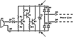
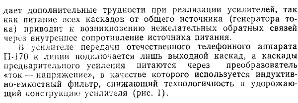
Sending amplifier of domestic telephone set P-170 has a line, to which is connected only output stage, and pre-amplifier stages are fed through current-voltage converter.
Inductance-capacitance filer is used as current-voltage converter (Fig.1). Using this filter lowers technological effectiveness and increases the cost of amplifier design.Ā
Fig. 1. Telephone set P-170. Circuit diagram.
Fragment. Sending amplifier:
Such sending amplifiers do not stand market competition with mechanoelectrical amplifier ¢ carbon microphone, which holds dominant position in popular models of telephone sets, despite its numerous shortcomings.
In this publication I describe a transistor two-terminal network - current modulator, deprived of shortcomings of the known sending amplifiers. It is designed for direct replacement (without redesign of telephone set circuit) of carbon microphones in telephone sets, both recent and old models.
Taking into consideration current nature of communications line as power supply, it is obvious to consider constancy of voltage drop on two-terminal network as behavior stability criteria, that is to use modulated voltage source (VS) as a sending amplifier.
Voltage source should meet the next requirements:
- Stability of amplification factor K and of steady component of voltage drop in wide range of line current;
- Symmetrical clipping of output signal at input overload to exclude appearance of even harmonics of signal;
- High efficiency, that is wide range of voltage drop changes, from doubled value of steady component to the value, close to 0;
- Absence of self-excitation;
- High technological efficiency of production and possibility of
microminiaturization. To do this, VS should tolerate for significant scattering of values of VS components, should not require any adjusting, should not contain any chokes, transformers and should contain minimal number of capacitors.
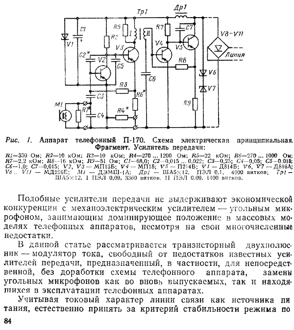
In Fig.2 it is shown VS made on the base of voltage stabilizer of parallel type. As it is shown, low-pass filter
(LPF), input source (IS) and capacitor are included into voltage feedback circuit (FC). Steady component of voltage drop on VS is held with high accuracy at the level, determined by stability voltage
(Ust) of stabilitron ST. Input signal causes voltage modulation, LPF excludes influence of FC in frequency range of the signal to be amplified.Ā
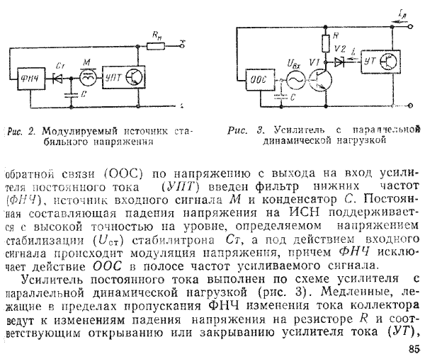
DC amplifier is designed based on circuit diagram of parallel dynamic load amplifier (Fig.3). Slow collector current changes are within transmission band of
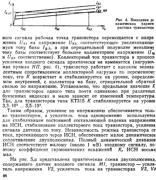
LPF. They lead to changes in voltage drop on resistor R and correspond to opening or closing of current amplifier (CA), which input is connected to resistor R through stabilitron V2. Changes in voltage drop on CA, making effect at transistor base V1 along circuit of FC, hold collector current at level, determined by formula IC = Ust / R. Collector current of transistor is stabilizing, and changes of base current under the impact of input signal are compensated with changes in collector voltage. Such compensation is determined by dependence of transistorÆs collector current on collector voltage (Fig.4). On positive half-wave of input signal, working point of transistor shifts from UC1 voltage to UC2, corresponding to increasing base current IB2. On negative half-wave higher collector voltage (IB3 and UC3 correspondingly) corresponds to the lesser base current. Collector current of transistor during amplification process is practically unchangeable (load line LL, Fig.4), transistor is functioning with high equivalent resistance of collector AC current load, its K is increasing and gets stabilized at the level, determined by internal (from collector to base) negative voltage feedback. It was found, that limiting K value for transistors of the same type is the same at different literal indexes and slightly depend on temperature. For transissotrs of KT315 type, K value is stabilized at level: (3.3 ¢ 3.5 ) .103.
Thus, voltage amplification is provided only by transistor. Current amplifier is simultaneously used for stabilizing of steady component of voltage drop on VS, stabilizing collector current of transistor, current amplifying of transducer signal. Independence of transistor mode on current, passing through VS, provides small dynamic resistance of two-terminal network. Full dynamic range os VS corresponds to low (about 1
millivolt) input signal, therefore harmonic distortions ration Kr of VS is extremely low.Ā
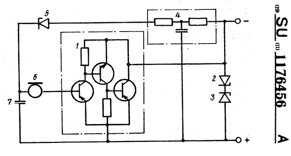
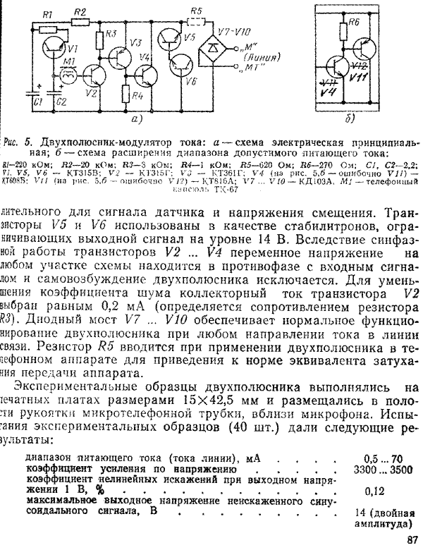
In Fig.5, it is shown working circuit diagram of two-terminal network, containing input signal transducer M1, transistor ¢ voltage amplifier V2. current amplifier on transistors V3, V4 (emitter junction of transistor V3, exhibiting sharp threshold properties is functioning as stabilitron on current amplifier input), LPF ¢ R1C1R2, stabilitron V1 (emitter junction, stability voltage 7V), capacitor C2, which performs functions of blocking stabilitron noise and separating transducer signal and voltage shift. Transistors V5 and V6 are used as
stabilitrons, limiting output signal at 14 V level. Because of in-phase operation of transistors V2 ģ V4, alternate voltage on any part of circuit is in counter-phase with input signal, and self-excitation of two-terminal network is excluded. To lower figure of noise (FN), collector current of transistor V2 is chosen to be equal to 0.2 mA (is determined by resistance of resistor R3). Rectifier bridge V7 ģ V10 provides normal functioning of two-terminal network at any current direction in communications line. Resistor R5 is included when using two-terminal network in telephone set for adjusting transmission loss equivalent to standard value.
Experimental samples of two-terminal network are conducted on Printed Circuit Boards of 15 x 42.5 mm size and were placed in hollow compartment of a handset receiver, next to microphone. Testing of experimental samples (40) gave the next results:
Range of feeding current (line current), mA 0.5 ģ 70
Voltage gain 3300 ģ 3500
Ratio of unlinear distortions at output voltage 1V, % 0.12
Maximal output voltageĀof undistorted sine-shaped signal, V 14 (pick to pick)
Noise level, adjusted to input, mkV, in frequency range, KHz
0.02 ģ 20 0.16
0.3 ģ 3 0.1
Dynamic resistance, Ohm, not more than 3
Dynamic range, dB 80
The obtained results prove the possibility of realize of two-terminal network modulator in microminiatured variant and its positioning (placing) in a body, similar to the body of standard carbon microphone, providing its
replaceability.
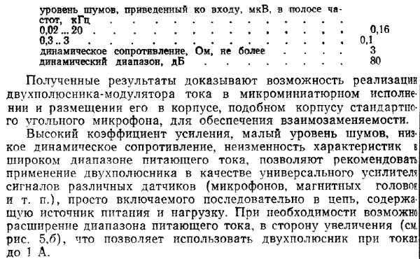
High amplification gain, low noise level, low dynamic resistance, non-changed parameters in wide range of feeding current allow to recommend two-terminal network as universal amplifier of signals from different transducers (microphones, magnetic heads etc), which are to be simply incorporated into circuit, containing power supply and load. Extension of the range of feeding current toward positive value is possible if necessary, allowing thereby to use two-terminal network at current values up to 1 A.
|